AD0xx-xx to AD7xx-xx
NVE Corporation 11409 Valley View Road, Eden Prairie, Minnesota 55344 USA
(800) 467-7141 Web: www.nve.com
Email: info@nve.com
11/15/02
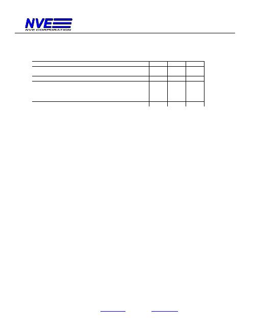
Absolute Maximum Ratings (NVE AD08x-xx):
Parameter
Symbol
Min
Max
Units
Supply Voltage
V
CC
7
V
Reverse Battery Voltage
V
RBP
-0.5
V
Current Sinking Output Off Voltage
33
V
Current Sinking Reverse Output Voltage
-0.5
V
Continuous Output Current
I
0
24
mA
Operating Temperature Range
4
T
A
-40
125
癈
Storage Temperature Range
T
S
-65
150
癈
Magnetic Field
5
H
None
Oe
Notes:
1.
Differential = Operate Point Release Point
2.
Minimum Release Point for AD0xx-xx to AD7xx-xx, except AD08x-xx, = 5 Oe. Minimum Release
Point for AD08x-xx = 3.5 Oe.
3.
Output current must be limited by a series resistor. Exceeding absolute maximum continuous output
current ratings will result in damage to the part. See the figure in the GMR Switch Product Selection
Guide for an output current derating curve.
4.
Thermal power dissipation for the packages used by NVE is 240癈/Watt for the SOIC8 package,
and 320癈/Watt for the MSOP8 and TDFN6 packages. See the Figure on Ambient Temperature vs.
Supply Voltage for derating information. Heat sinking the parts by attaching them to a PCB
improves temperature performance.
5.
There is no maximum magnetic field that will cause damage to the device.
6.
If V
CC
>6.6V, V
REG
=5.8V. If V
CC
<6.6V, V
REG
= V
CC
0.9V.
发布紧急采购,3分钟左右您将得到回复。
相关PDF资料
ADL024-14E
DIGITAL SWITCH 55HZ ULLGA
AFL300-00
SWITCH MAGNETIC DIG 5.5V 8MSOP
AH173-WL-7-A
IC HALL SENSOR LATCH 25MA SC59-3
AH175-PL-B-B
IC HALL SENSOR BIPO LATCH SIP-3L
AH1751-PG-A-A
IC HALL SENSOR LATCH SIP-3
AH180-PL-A
IC SENSOR SWITCH HALL SIP-3L
AH1801-SNG-7
IC HALL SWITCH CMOS 6-DFN
AH1802-FY4G-7
IC HALL EFFECT SENSOR 3-DFN
相关代理商/技术参数
ADH025-00E
制造商:NVE Corporation 功能描述:IC DIG SW MAGNETIC 30 V MSOP-8 制造商:NVE Corporation 功能描述:IC, DIG SW, MAGNETIC, 30 V, MSOP-8 制造商:NVE Corporation 功能描述:IC, DIG SW, MAGNETIC, 30 V, MSOP-8, MSL:-, Digital IC Case Style:MSOP, Hall Effe
ADH20010
制造商:ZETTLER MAGNETICS 功能描述: 制造商:ZETTLER Magnetics Inc 功能描述:Power Transformer 2500Vrms Dual Prim. Dual Sec. 230V/115V Prim. 10V/5V Sec. Through Hole
ADH200120
制造商:ZETTLER Magnetics Inc 功能描述:
ADH20016
制造商:Zettler Magnetics 功能描述:ADH Series 16 VCT 0.07 A Split Bobbin Design Precision Molded-in Terminals
ADH20028
制造商:Zettler Magnetics 功能描述:1.1VA 50/60Hz Radial Power Transformer
ADH20048
制造商:Zettler Magnetics 功能描述:POWER TRANSFORMER, 1.1VA 50/60HZ
ADH2400IAA5DOS
制造商:Advanced Micro Devices 功能描述:E64 IC OPN - Trays
ADH25
制造商:MITA 功能描述:P.V.C. ADHESIVE
